The 250407 was the most common breadbin motherboard Commodore ever shipped. If you’re working on one, the question that comes up over and over again is “which chip is that one?” — because every C64 symptom guide on the internet refers to chips by their U-number, and the U-numbers move around between revisions.
These five diagrams cover everything on a 250407. They’re meant to be used alongside Ray Carlsen’s chip-vs-symptom guide — Carlsen tells you which chip is failing; these diagrams tell you where on the board to find it.
The U-numbers on these diagrams use the canonical Commodore numbering for the 250407 (schematic 251138). They will not line up with the 250425, the 250466, or any of the short boards — those have their own layouts.
Ports
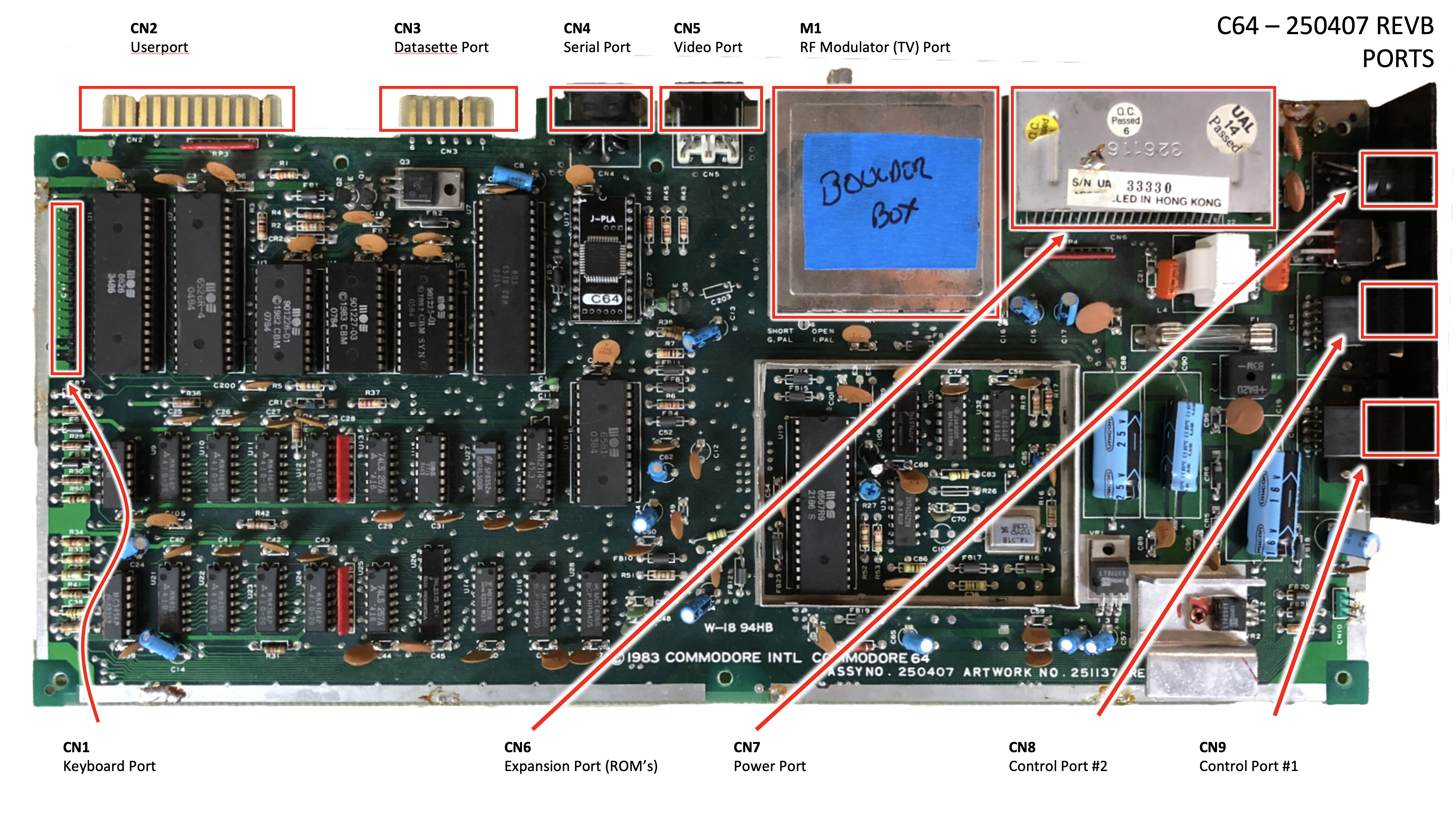
Every port on the back, side, and underside of the case lands on the motherboard at one of these positions.
- CN1 — Keyboard port (24-pin header along the front-left edge, mates with the keyboard cable)
- CN2 — User port (the 12/24 edge connector at the back-left, RS-232 / general I/O)
- CN3 — Datasette port (6-pin edge connector, Commodore tape drive)
- CN4 — Serial port (6-pin DIN, IEC bus to 1541s and printers)
- CN5 — Video port (8-pin DIN, separate luma/chroma plus composite and audio)
- CN6 — Expansion port (44-pin edge connector along the bottom, cartridges and diagnostic cartridges plug in here)
- CN7 — Power port (7-pin DIN, +5V regulated and 9V AC from the brick)
- CN8 — Control port #2 (DE-9, joystick or paddle)
- CN9 — Control port #1 (DE-9, joystick, paddle, light pen, or mouse)
- MJ — RF modulator (TV) output, on the modulator can on the right side of the board (Astec or Mitsumi, depending on production run)
Custom chips and RAM
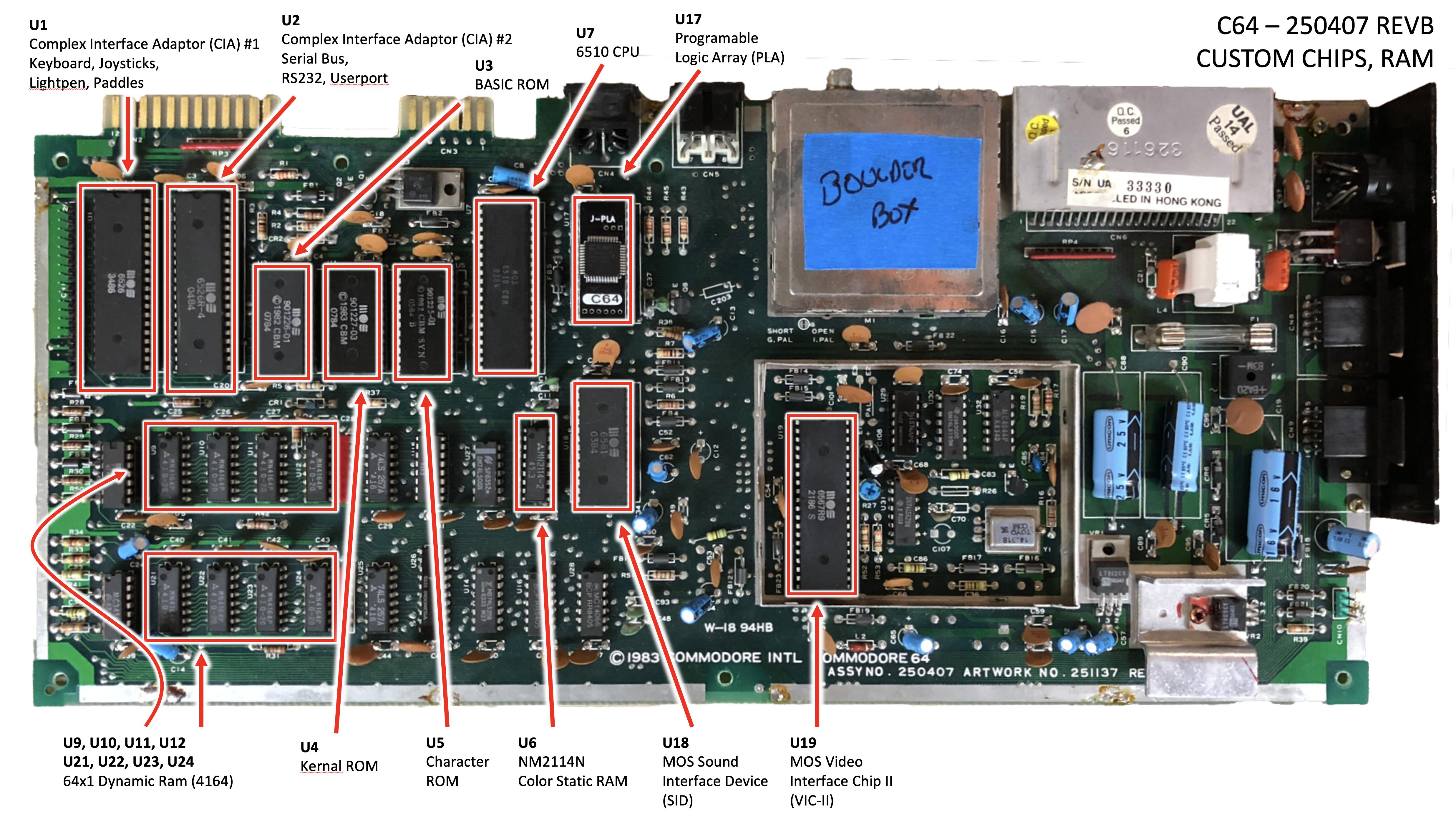
Almost every chip on this diagram is an MOS part, custom-designed for Commodore. Most C64 failures hit one of these.
- U1 — 6526 CIA #1 (Complex Interface Adapter): keyboard scanning, joystick ports, lightpen, paddles. One of the more common failure modes on the breadbin.
- U2 — 6526 CIA #2: serial (IEC) bus, RS-232, user port. Same chip as U1; symptoms are different because of what it’s wired to.
- U3 — BASIC ROM (901226-01), 8 KB.
- U4 — KERNAL ROM (901227-03), 8 KB. Holds the boot routines, screen editor, and I/O drivers.
- U5 — Character ROM (901225-01), 4 KB. The built-in PETSCII glyphs.
- U6 — MM2114 color static RAM, 1Kx4. Stores the 4-bit color value for each character cell.
- U7 — 6510 CPU. The 6502 core with an extra 8-bit I/O port (six bits brought out on the C64) wired to the cassette and banking lines.
- U17 — 906114-01 PLA (Programmable Logic Array). Address decoding and bank switching. Notoriously fragile and infamously hard to source — the most-faked chip on eBay.
- U18 — 6581 SID (Sound Interface Device). Three-voice analog synthesis with filter.
- U19 — 6567 VIC-II (Video Interface Chip II, NTSC; PAL boards use the 6569). Sprites, raster timing, and video output.
- U9, U10, U11, U12, U21, U22, U23, U24 — eight 4164 DRAMs (64Kx1), arranged in two rows along the bottom. Together they make up the 64K of main RAM.
Glue logic, part 1
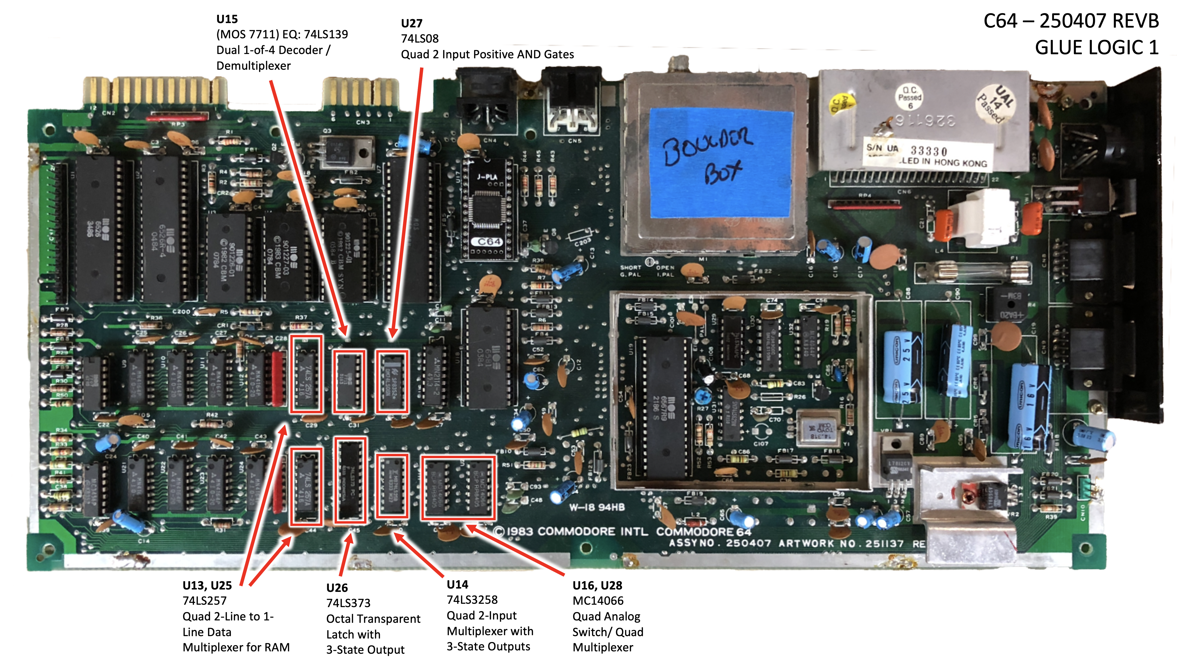
The 74-series TTL parts that wire the custom chips together. None of these are particularly rare — all of them can be sourced cheaply from any electronics supplier.
- U13, U25 — 74LS257, quad 2-line to 1-line data multiplexer. Used to multiplex the address lines into the 4164 DRAMs (which expect a row address and a column address on the same pins).
- U14 — 74LS373, octal transparent latch with 3-state outputs. Latches the VIC-II’s address lines.
- U15 — 74LS139 (sometimes marked with a Commodore house number — 7708 or 7711, depending on the source — on later boards), dual 1-of-4 decoder / demultiplexer. Chip-select decoding.
- U16, U28 — MC14066 / 4066, quad analog switch (quad bilateral switch). Used for signal routing between the VIC-II and CPU bus cycles.
- U26 — 74LS258, quad 2-input multiplexer with 3-state outputs. More address-line multiplexing.
- U27 — 74LS08, quad 2-input positive AND gates. General-purpose glue.
Glue logic, part 2
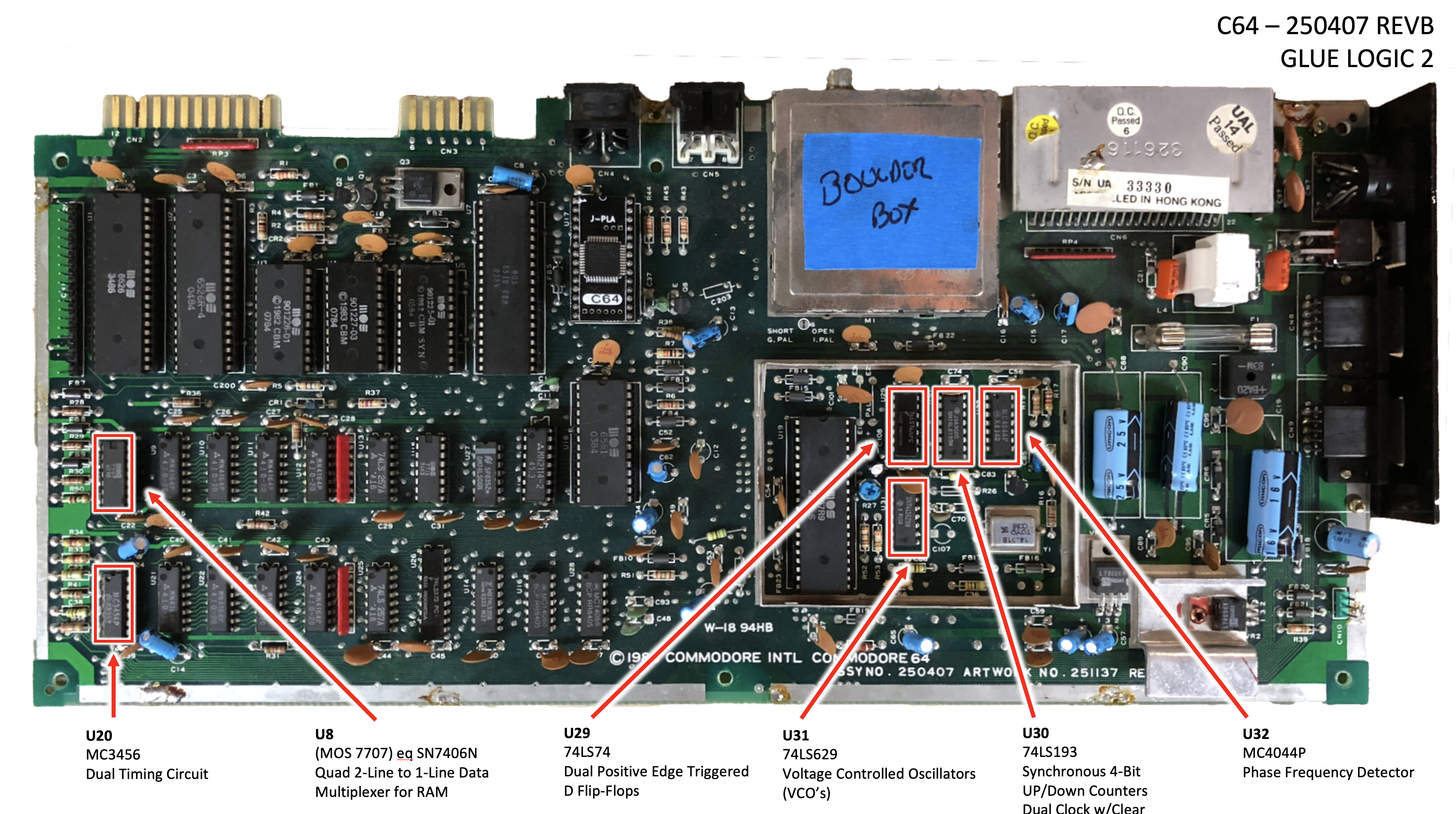
The second half of the 74-series logic, plus the clock-generation chain that feeds the VIC-II and the CPU.
- U8 — MOS 7707 (functionally equivalent to SN7406 / 74LS06), hex inverter buffer / driver with open-collector outputs. Drives various signal lines that need open-collector wiring.
- U20 — MC3456 dual timing circuit (a dual 555). Part of the paddle-input timing path that feeds the SID’s POT X / POT Y pins.
- U29 — 74LS74, dual D-type positive edge-triggered flip-flops.
- U30 — 74LS193, synchronous 4-bit up/down binary counter with dual clock and clear.
- U31 — 74LS629, voltage-controlled oscillator (VCO).
- U32 — MC4044P, phase-frequency detector. U30/U31/U32 together form the phase-locked loop that generates the dot clock from the color subcarrier.
Analog
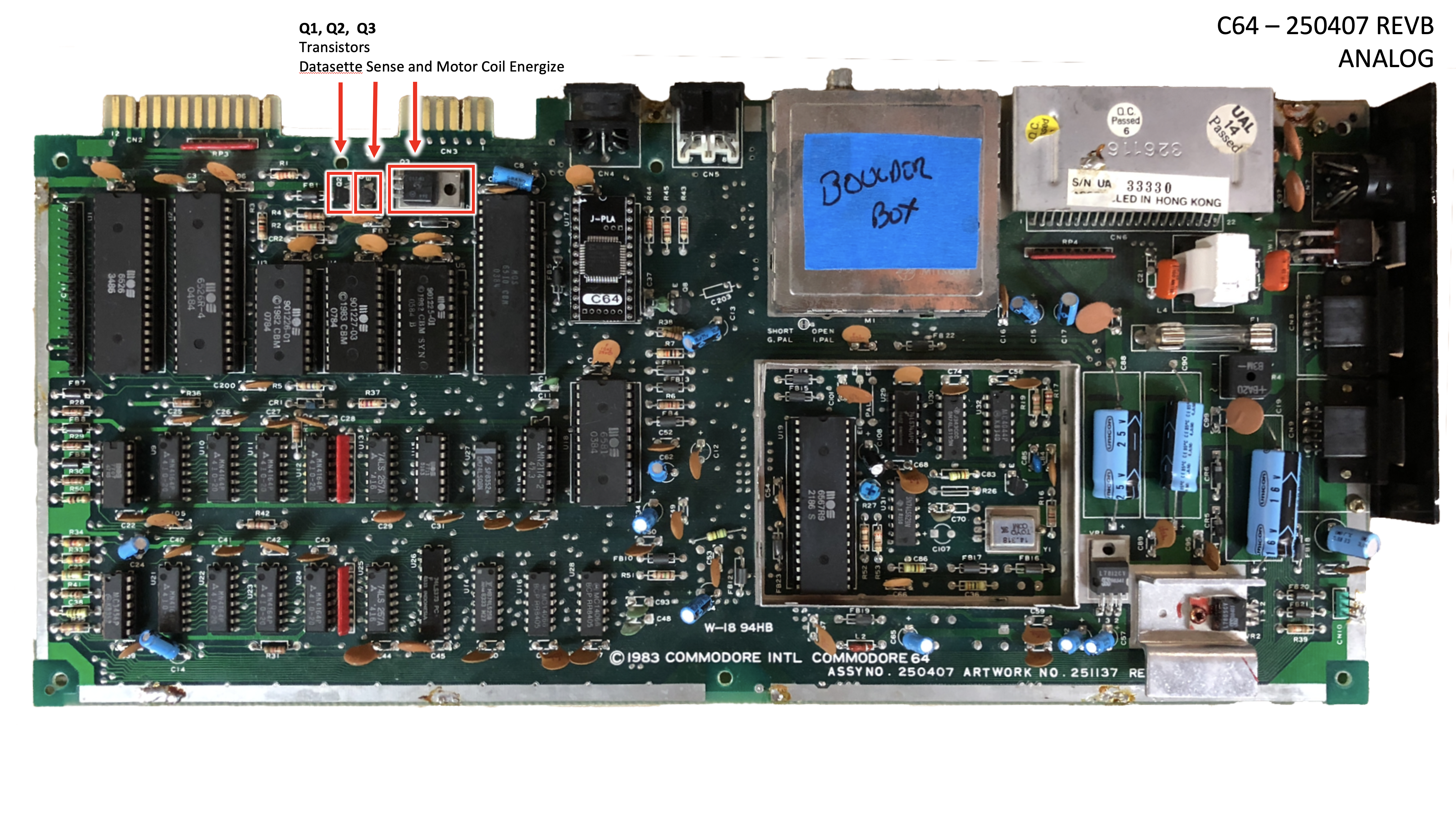
Most of the analog work on the C64 is hidden inside the SID and VIC-II. What remains as discrete components on the board is the datasette interface and a handful of small-signal transistors.
- Q1, Q2, Q3 — small-signal transistors that drive the datasette read/write/sense lines and energize the cassette motor coil. These rarely fail, but if your datasette won’t move tape this is where to start checking.
How to use this with the symptom guide
The standard repair flow on a 250407 looks something like:
- Power supply first — measure +5V at the user port before you do anything else. If the brick is bad, fixing chips is pointless.
- Dead-test cartridge in the expansion port (CN6). The dead-test points at chips by U-number.
- Look up the U-number against Carlsen’s symptom guide.
- Find that U-number on the diagram for the right page above (custom chips and RAM live on page 2; glue logic is split across pages 3 and 4).
- Pull the chip, socket it on the way back in, move on.
A worked example of this flow is in the Commodore 64 restoration write-up, which used these exact diagrams to track which chips needed replacing.
Useful Documents
C64 Diagnostic Instruction and Troubleshooting Manual (PDF) — Commodore’s official diagnostic manual (part 326070-01). The factory reference for board-level fault isolation, dead-test cartridge procedures, and chip-by-chip symptoms — the deeper companion to Carlsen’s symptom guide.
C64 Service Manual (PDF) — Commodore’s official service manual for the breadbin. Schematics, board layouts, parts lists, and disassembly procedures — the reference for any work past chip-swapping.
How to Identify Your C64 Board — Ray Carlsen’s guide to identifying which of the half-dozen breadbin motherboard revisions you have. The first thing to confirm before using these diagrams — the U-numbers on this page only line up with a 250407.